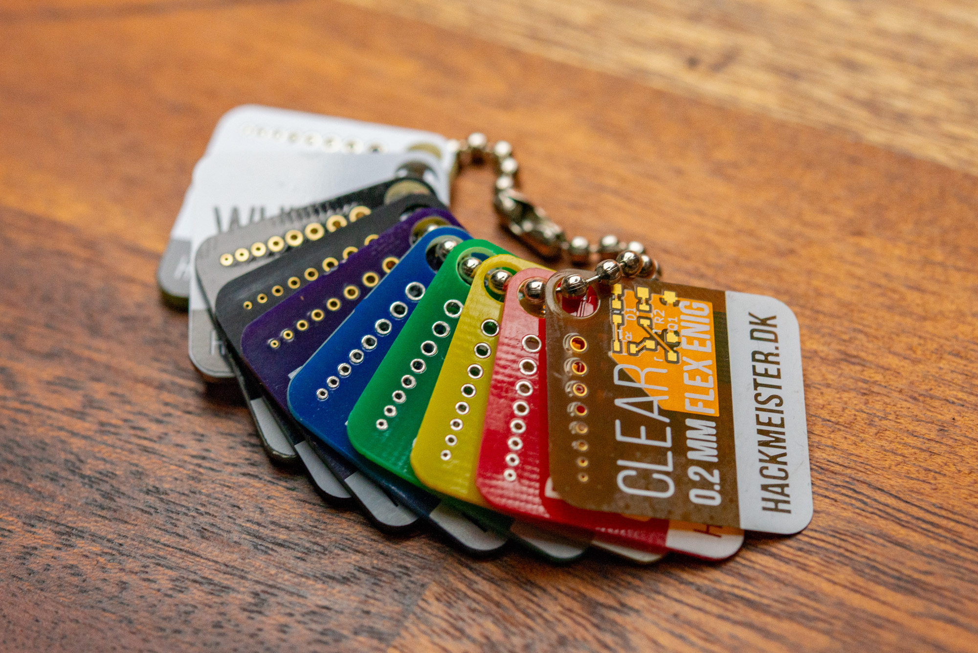
PCB Color, Thickness and Material Samples
For the past many years, green solderstop has been the standard in PCB production and most cheap manufacturing companies have had it as the defualt color and many still do. The green color specifically has been optimized over many years and it is likely the one where you will get the best yield in a larger manufacturing run. For smaller, maybe even hand assembled runs, this will likely be less important.
When working on projects where the PCB is visible, that being either development boards, that is most often used without a case or the more and more common artform that is electronic conference badges, the visual appearance is of greater importance and the PCB is in many aspects a type of canvas for graphics.
When doing graphic design and print production, designers often use tools like Pantone color books or paint samples and this projects is attempting to make such a tool, but specifically for PCB designers.
I have started out with just a few standard color samples and then added a few more of the special cases. Some manufacturers have more options than what I have listed below and there is also a difference between different companies, so when you order red from one supplier, it’s not necessarily the exact same color as red from another one. Some have a much more orange red, some a deeper red, almost towards carmine.
For exact matches in a production, especially with special colors, I would always recommend to do a prototype run and check with the factory, that the prototype run and the production run is done with the same specs. Small and quick prototype runs are often processed using different machines compared to a medium run of eg. a few hundred PCBs.
Design of the samples
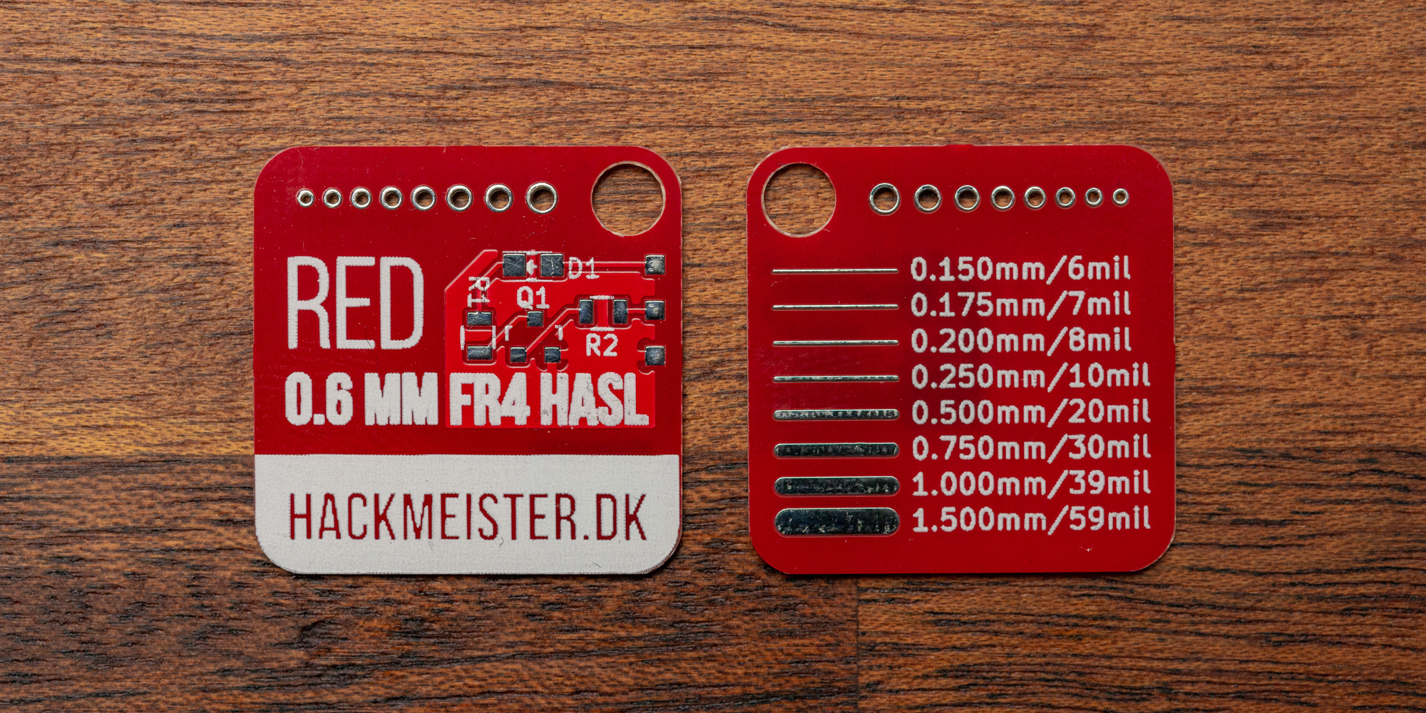
These samples have a front side, which is primarily silkscreen artwork, and a backside that includes various footprints and other usefull stuff when designing PCBs, like hole sizes, text sizes, pad spacing or trace widths.
The text on the front is artwork imported into KiCad via the bitmap importer. The artwork originated in Adobe Illustrator and was exported as a black and white PNG file, before it was imported as a footprint and placed on the board.
Everything else was made inside KiCad. The small circuit on the front has a copper pour, so that silkscreen is printed both where there is copper and where there is none.
In cheaper production, the silkscreen will often be a little bigger than what was defined. This is mostly seen when having inverted text like in the bottom of each of these samples, where the letters gets thinner. If you don’t use a somewhat bold font, you risk letters dissapearing.
Standard colors
The standard colors are available from most of the companies in China and in most cases, you can also get the 6 differrent thicknesses ranging from 0.6mm to 2.0mm total thickness.
All the standard color PCBs in this post are from DirtyPCBs, they are FR4 base material and made a few years ago. The silkscreen quality for these are decent for a cheap board, but they are not as clear as the more expensive options. If you look at the letters “M” and “A” you will see jaggered edges.
0.6mm is pretty thin and if you only need a slight curvature, you could probably use 0.6mm PCBs and bend it a little, though if you bend it too much, it will break. The PCB will also try to straighten out, so you would need to attach it to something to keep the shape.
Red solderstop is usually paired with white silkscreen. There are commpanies that will allow you to choose other silkscreen colors, but white will likely give the best contrast.
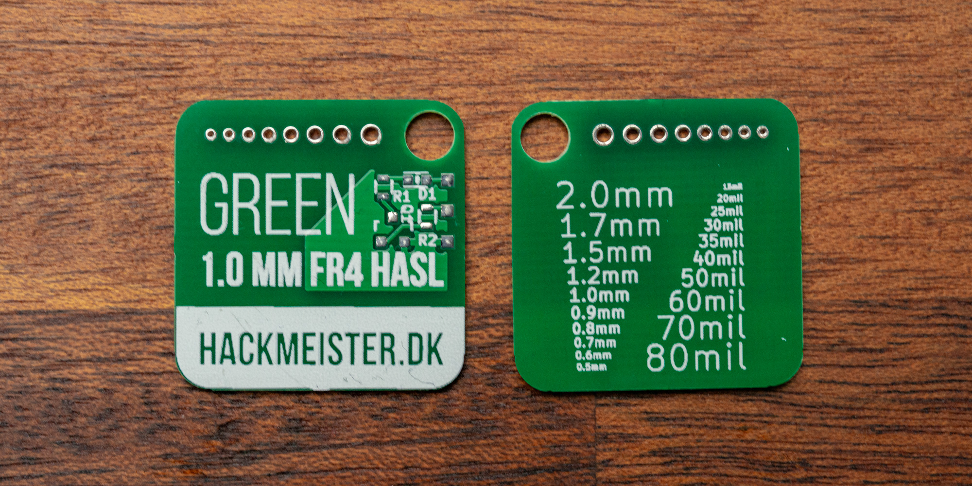
The backside of this sample shows different trace widths and an approximated calculation between mm and mil.
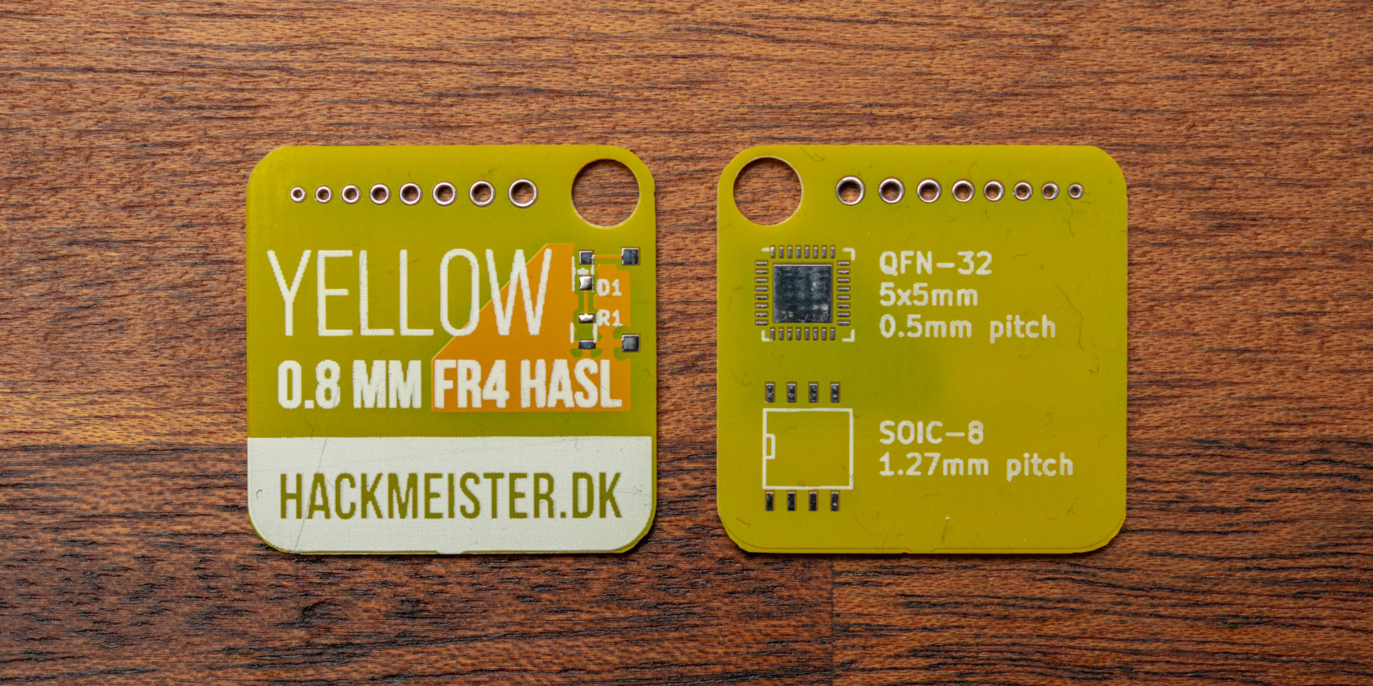
0.8mm is pretty close to the same thickness as a creditcard (just the plastic, not the raised numbers and letters), and connectors like male USB Type C often require this thickness since they connect on both sides of the PCB, with half of the connections on each side.
The traces are usually very visible with yellow solderstop and you would think that black silkscreen would be the default, but most places will give you white silkscreen on top of yellow solderstop.
This sample has a few common chip footprints on the back. Many smaller flash chips come in a SOIC-8 house.
1.0mm thickness is starting to get quite sturdy. Mini PCIe cards for laptops and similar are usually 1.0mm thick, since that is what the socket is designed for and for small boards like a mini PCIe card, there will be very little flex.
As mentioned earlier, green solderstop is the most common and often the cheapest and it is almost always paired with a white silkscreen.
It is usually possible to follow a trace under the green solderstop, as the copper will show up a bit lighter than the green directly on top of the FR4.
On this sample I have included different text sizes, so that you can see how small is too small. These are the standard texts in KiCad, only the size has been changed.
1.2mm can be used if you want a slightly thinner board, but still want it to be somewhat stiff. For smaller boards, 1.2mm will likely work very similar to 1.6mm.
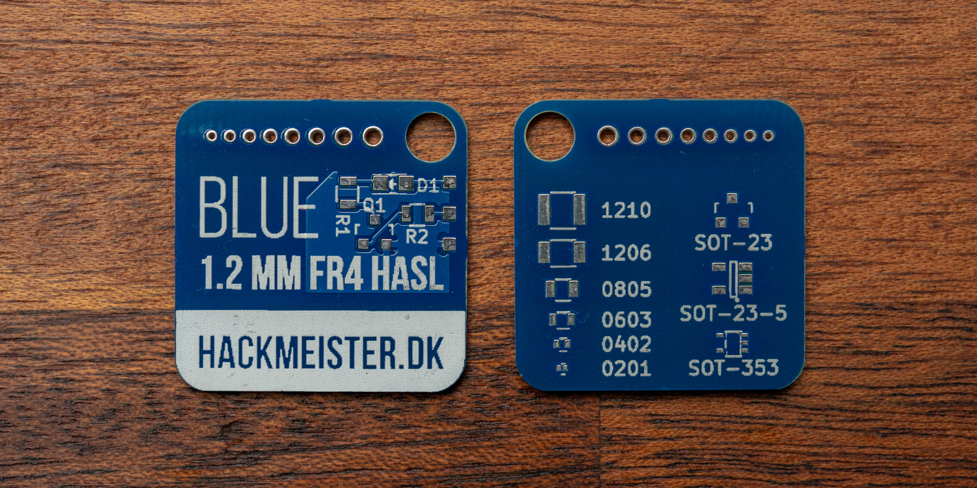
The blue solderstop with white silkscreen got kind of popular with the Arduino boards about 10 years ago and a lot of little cheap breakout boards from China uses blue solderstop. It’s a little bit more difficult to follow the traces under the blue solderstop, but not impossible.
This is again a few common footprints for resistors and capacitors and a few most often used for transistors and voltage regulators.
The 1.6mm is usually the default and will, in most cases, provide a sturdy base for components and connectors. Even sections that are only a few millimeters wide (like the part around the mounting holes) will not break off, but if you have a thin 1mm section between two larger sections (often used when panelizing), you can still break it without tools.
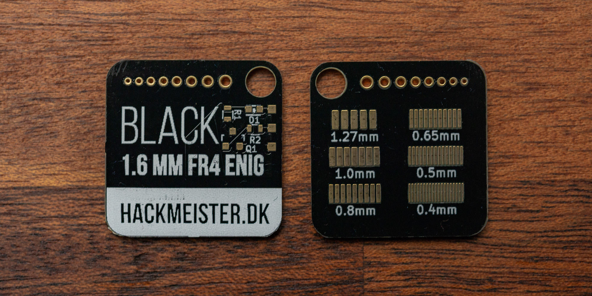
Black solderstop normally covers the traces and if you need to follow a trace, you have to rely on the thickness of the copper to give you clues as to where the traces go. Black solderstop is almost always combined with white silkscreen, though there are a few exceptions, but beware, even though a company will sell you a combination, it might not look like you expect, since some of the silkscreen colors are so thin, that they can’t brighten the black color and therefore you will end up with a very dark silkscreen and sometimes almost black.
Where all the previous samples have used HASL (Hot Air Surface Leveling), this sample have an ENIG (Electroless Nickel Immersion Gold) finish of all the pads. This finish is much more even and flat, compared to HASL and only exist in a RoHS compliant version, where you can get HASL both with and without lead.
The backside of the black sample is for checking the pin spacing of differrent chips. Holding the legs up to one of these will quickly make it clear what spacing is used.
The 2.0mm thick PCBs are quite hefty and most fabhouses will charge you extra for this tickness. If you need the mechanical strength it might make sense or if you want to make a male USB-A connector purely in PCB, 2.0mm is the one to get.
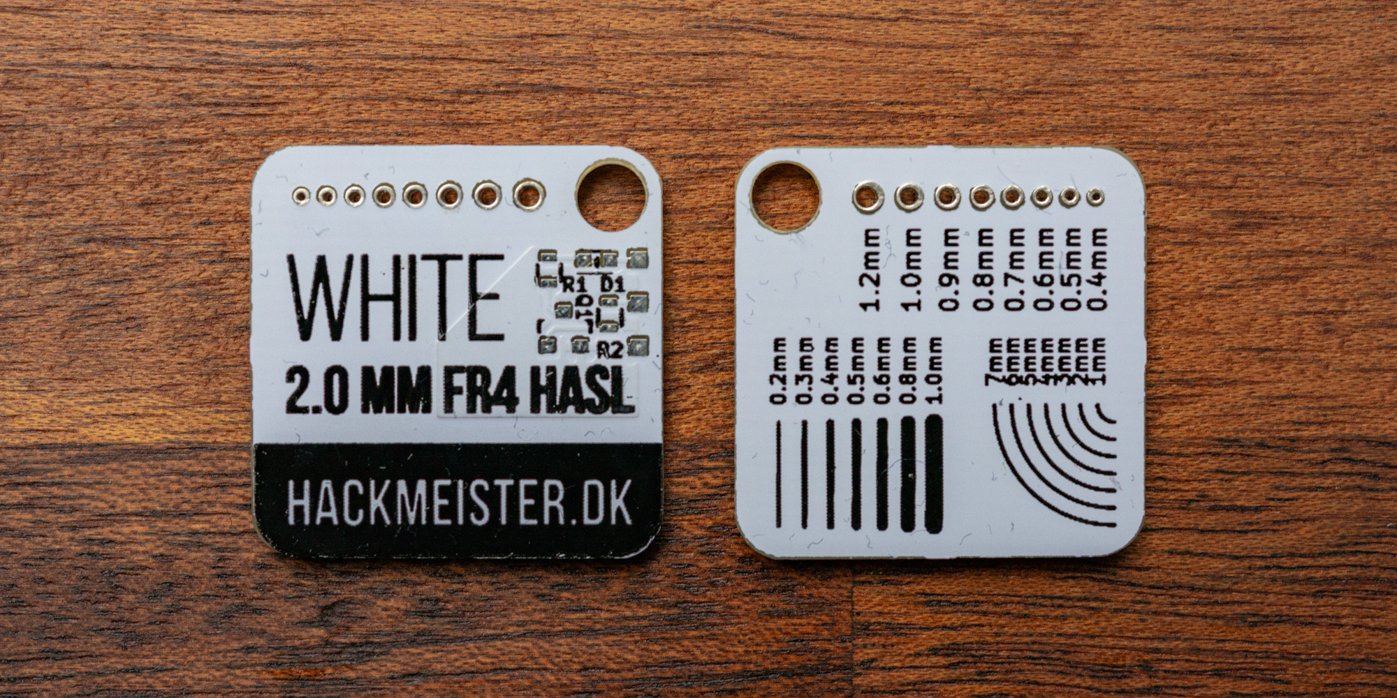
Similar to the black solderstop, the white will also cover the copper pretty good. Both black and white are often used with LED lights to minimize false color cast of the light. White solderstop is primarily combined with black silkscreen, whick gives you a very high contrast and since you can’t really see the traces, a very binary black and white look.
There are board houses that can use colored silkscreen on white solderstop, and unlike the black solderstop, it works a bit better.
On the backside of this sample you will find the legend for the plated holes found on all of the above samples and in addition there are also silkscreen line thicknesses and different radii, to help you make nice rounded corners.
Aluminium substrate
Aluminium substrate is an option, where the FR4 fiberglass is replaced with an aliminium plate. These are most often used when you need to transfer heat away from a component eg. in LED lighting or similar.
Since the base material is conductive, these are only single layer circuits and there are no plated via connections, though you can make mechanical holes for mounting or similar.
There is a thin layer of non conductive material between the alumminium substrate and the copper traces, so that the traces are not shorted through the aluminium.
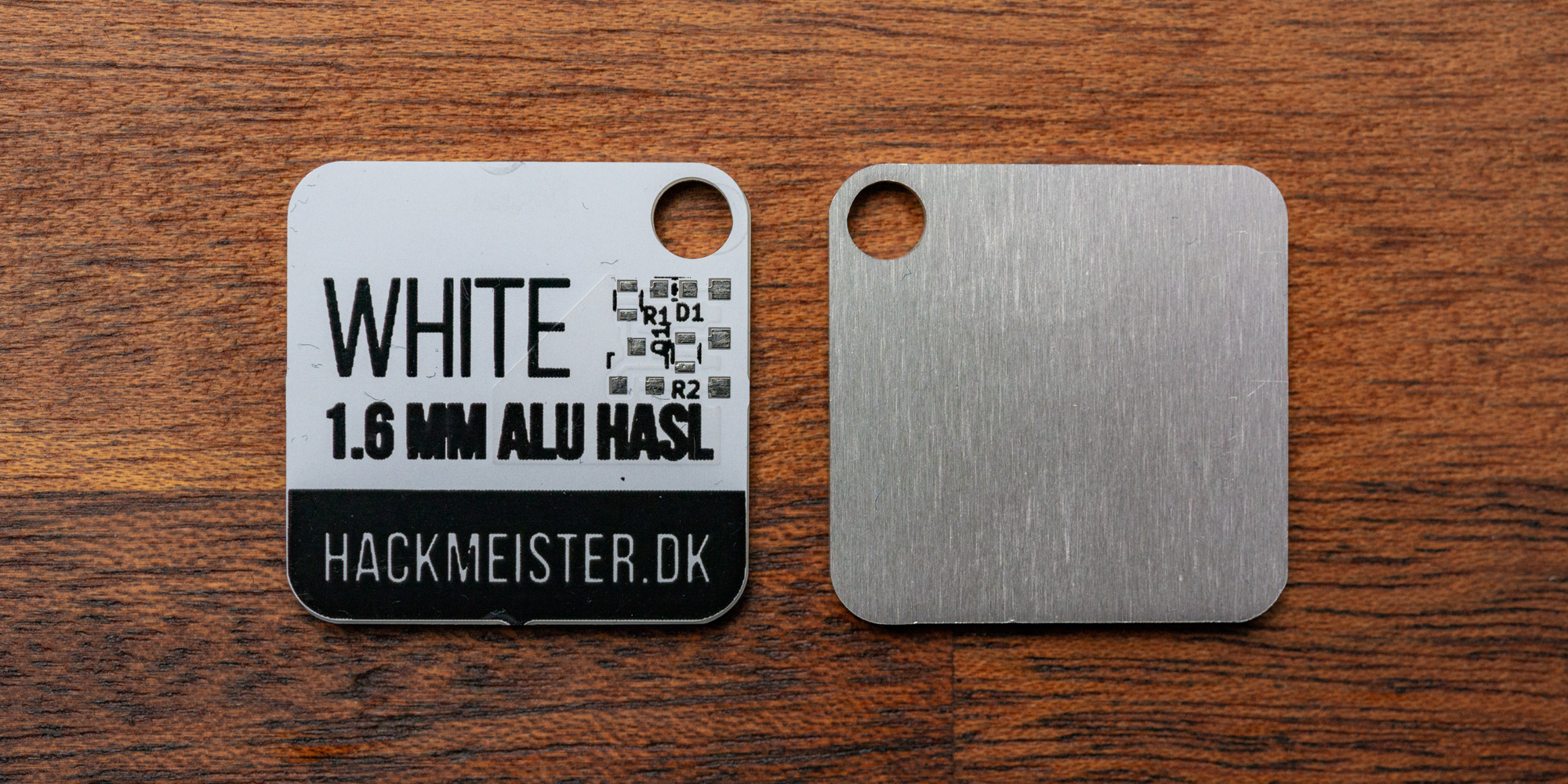
This sample is made by AllPCB and white solderstop was chosen since that will likely be the most used combination with eg. LED modules.
Since this is a single layer board, the back of this sample is the raw anodized aluminium.
OSHPark specialty
OSHPark is a company in the US, that has specialized in small orders (minimum amount is just 3 pcs.) and a very high quality. For a long time, all they offered was purple soldermask, white silkscreen and ENIG finish, but they have gotten a few new offerings lately.
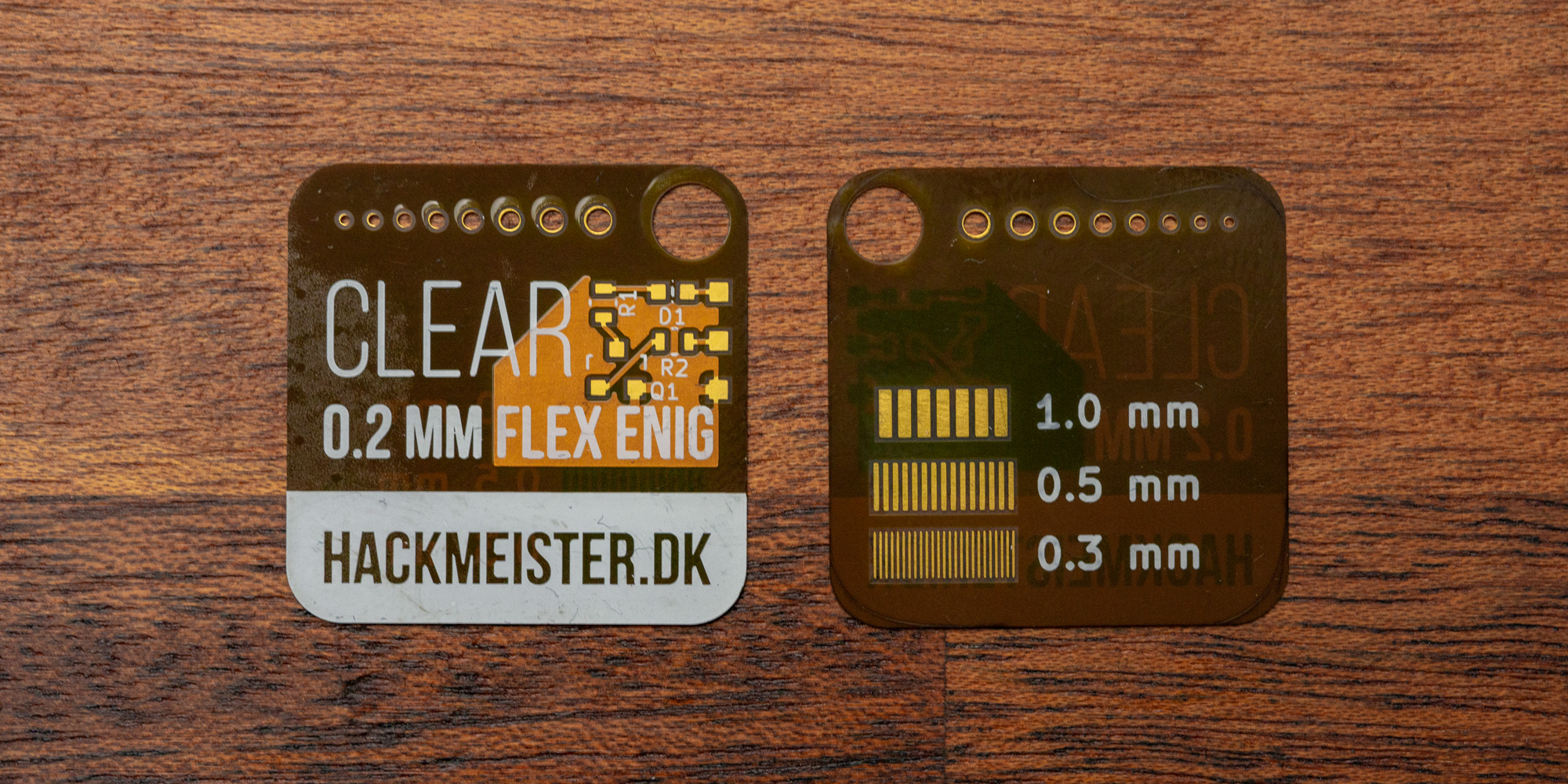
Flex PCBs uses a very thin film instead of the FR4 base material and with an overall thickness of only 0.2mm, these can be used for some very interesting origami style electronics. Flex has usually been a bit expensive to get started with, but the offerings from OSHPark is opening up for a more affordable option, for smaller flex projects. These are two layers and the solderstop is clear, making it pretty easy to follow the traces in a debug scenario. You can even see the traces from the back, if you haven’t covered it up with the bottom layer copper. The silkscreen on these are very sharp, and board outline has a very clean cut.
The backside on this sample is similar to the black sample above, but with an even smaller spacing of just 0.3mm. The top has been left blank to emphasize the transparent nature of the flex PCBs.
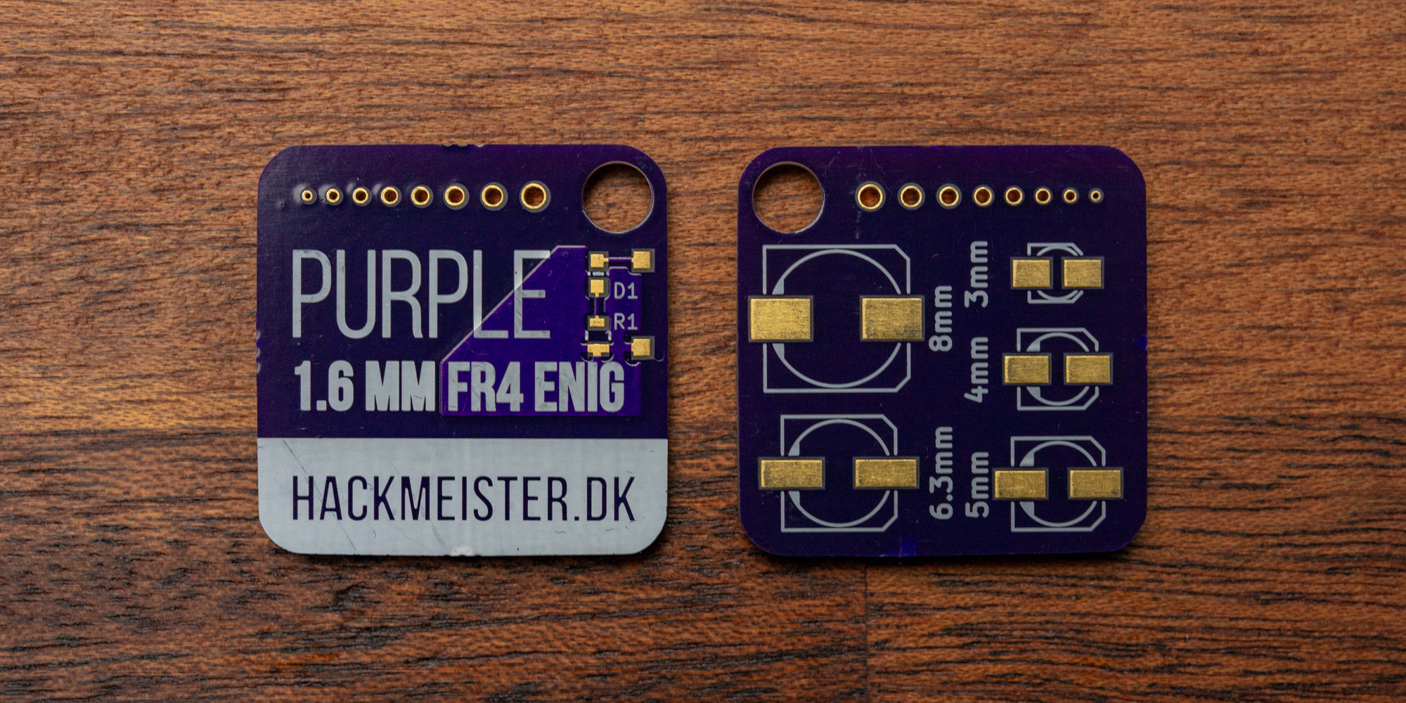
This is the classic purple OSHPark signature color and like the flex PCBs, the silkscreen is very sharp and detailed. These have ENIG finish and are therefor always RoHS compliant.
The purple sample has a series of electrolytic capacitors on the back. These are just the smaller ones, but they are really difficult to solder if you chose a footprint that is too small.
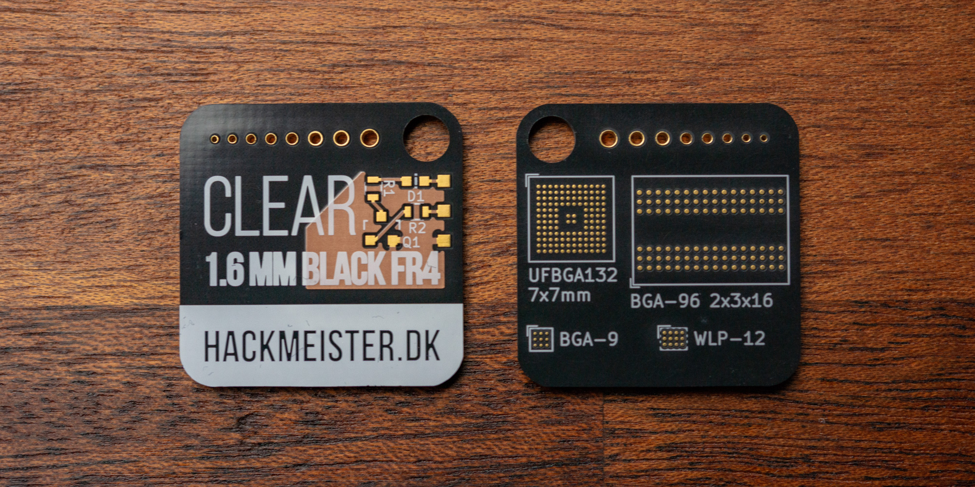
This is the latest combination from OSHPark and it is black FR4 base substrate with clear soldermask and white silkscreen. Similar to the flex PCBs, you see the traces very clearly and where the regular FR4 will diffuse light shining through, this black FR4 will not let any light through.
To showcase some of the capabilities of OSHPark, the backside of the Afterdark sample has a few common, fairly dense BGA footprints.
Source files and shared projects
All of the KiCad design files and the artwork files (Adobe Illustrator format) are available in the following repository on GitHub:
For the 3 OSHPark samples, I have made shared projects to make it super easy to order, just make sure you select the correct type, when checking out: